Semiconductor Etch Equipment Market Size, Share & Industry Analysis, By Etch Type (Dry Etch and Wet Etch), By Dimension (2D, 2.5D, and 3D), By Application (Semiconductor Fabrication Plant/Foundry, Semiconductor Electronics, and Test Home), and Regional Forecast, 2026-2034
Semiconductor Etch Equipment Market Size
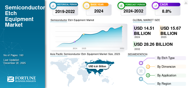
The global semiconductor etch equipment market size was valued at USD 15.67 billion in 2025 and market is projected to grow from USD 16.95 billion in 2026 to USD 34.07 billion by 2034, exhibiting a CAGR of 9.10% during the forecast period. The Asia Pacific dominated global market with a share of 66.50% in 2025.
Semiconductors are complex products that are hard to design and need complex operations to produce. Semiconductor etch equipment is a prime processing equipment that performs 50-60% of the operations. These machines are involved in the finishing phase of the product, where wafer surfaces are leveled with two etching operations: dry etch and wet etch. These machines are majorly adopted in industries, such as semiconductor fabrication plant/foundry, semiconductor electronics manufacturing, and test homes.
Download Free sample to learn more about this report.
The global market is growing progressively due to heavy investments by global tech giants to facilitate in-house semiconductor manufacturing and easy sourcing. The demand for semiconductor etch equipment is set to grow in line with the demand for manufacturing equipment owing to the rising need for wafer sizes with 2.5 and 3D dimensions in modern computing and electronic devices.
The COVID-19 pandemic caused a major decline in the market’s growth in 2020 and a significant decrease in the demand for semiconductors due to lockdowns that interrupted semiconductor supply. Post Q2 2020, the semiconductor industry is on the rise owing to higher demand for semiconductors in advanced computing, connected devices, remote healthcare, and modern logic operations, highlighting the importance of these components in today's economy.
Semiconductor Etch Equipment Market Trends
Technological Advancements and Rising AI Implementation to Drive Product Adoption Trend
Globally prominent players in the industry are focusing actively on research and development with hefty investments and creation of advanced technologies that can manufacture more compact wafers. Semiconductor etch equipment has a prominent application across the industry as a material removal machinery that levels the wafer surface for the easy installation of semiconductor components in electronic devices. These components are majorly used in growing telecommunication technologies, such as 4G, 5G, and fiber optic networks. The machines offer high accuracy and effective production rates. Post-pandemic, they have been used in wafer processing for technological advancements, such as Artificial Intelligence (AI) and Industry 4.0. These advancements improve business growth and profit margins for manufacturers, which will drive the product’s adoption among end users.
- For instance, in April 2024, the President of South Korea announced that the government would invest USD 6.94 billion in AI in the next three years as the country focused on retaining its lead position in the global semiconductor market. Also, as part of the investment, the government will set up a USD 1 trillion fund to help AI chipmakers in the country grow.
Semiconductor Etch Equipment Market Growth Factors
Increasing Semiconductor Demand and Miniaturization of Wafers to Bolster Market Growth
Globally, the demand for advanced semiconductor chips, IC chips, logic circuits, and other wafers is increasing at a commendable pace across industries, such as EV, connected device, consumer electronics, and home appliance. In addition, the growing emphasis on miniaturization of wafers by key industry players for various end-use applications has bolstered the demand for semiconductor etching. The miniaturization of wafers and chips supports precision engineering and delivers compact devices to end users at minimal cost. Thus, compactness and miniaturization are the potential factors that will drive the demand for semiconductor etch equipment in the long term.
- For instance, in June 2024, Intel Corporation planned to invest around USD 100 billion to construct a new semiconductor fabrication plant in the U.S. states, including Ohio, Arizona, New Mexico, and Oregon.
RESTRAINING FACTORS
Heavy Initial Investments and Late ROI to Hamper Product Demand
A semiconductor machinery is a huge asset for the company and demands a large capital investment. However, the Return on Investment (ROI) for the manufacturers is quite long. These machines are efficient in performing complex material removal operations with minimal process time, which is highly demanded in the production lines. However, the initial setup cost is a prime hindrance for medium-scale enterprises and start-ups and can hamper the demand for etching equipment in the short term.
Semiconductor Etch Equipment Market Segmentation Analysis
By Etch Type Analysis
Demand for Dry Etch Equipment to Grow Due to Better Control & Safety During Wafer Manufacturing
Based on etch type, the market is segmented into dry etch type and wet etch type.
The dry etch type segment is set to acquire the highest market share. Dry etching provides more control over the etching process with strong isotropic control and is generally safer than the traditional etching methods. It also uses gas in place of costly chemicals, which helps minimize production loss and maximize profits and efficiency.
The wet etch type segment is also set to grow steadily owing to sturdy production lines and frequent demand for wet etch chemical processing in traditional chip manufacturing processes. The segment acquired 56.70% of the market share in 2026.
To know how our report can help streamline your business, Speak to Analyst
By Dimension Analysis
3D Segment to Showcase Highest Market Share Due to Strong Demand for Wafer Miniaturization
Based on dimension, the market can be categorized as 2D, 2.5D, and 3D.
The 3D segment is set to attain the largest semiconductor etch equipment market share owing to minimal machining cost and high demand for more miniaturized and compact wafers in telecommunication and broadcasting devices. Also, 3D semiconductor etch equipment provides excellent finishing to the wafer and semiconductor surface with effective material removal and delivery of the thinnest and most proficient chips. The segment is likely to hold 41.95% of the market share in 2026.
The 2.5D segment is set to grow steadily with stable demand for this equipment in IT hardware and telecom components manufacturing. The segment is expected to display a CAGR of 9.1% during the forecast period. Also, the slow growth of 2D semiconductor etch equipment is due to lesser use of this technology in modern wafer manufacturing as manufacturers are upgrading to advanced 2.5 and 3D technologies.
- For instance, in December 2023, Hitachi Hi-tech Corp. announced the launch of its GT2000 high-precision electron beam metrology system. GT2000 uses the Hitachi Hitech technology and expertise in CD-SEM. The device is equipped with a new detection system for futuristic 3D semiconductor devices. It also uses low damage, high-speed multi-point measurement functions for the imaging of High-NA-EUV resist wafers.
By Application Analysis
Semiconductor Fabrication Segment Dominates Market Owing to Rising Circuit Demand from Manufacturing Sector
Based on application, the market is classified into semiconductor fabrication plant/foundry, semiconductor electronics, and test home.
The semiconductor fabrication plant/foundry segment is acquiring the highest market share due to the growing demand for semiconductors and high investments across industries, such as consumer electronics, medical devices, and automotive. The segment is projected to hold 58.05% of the market share in 2026.
Furthermore, semiconductor electronics manufacturing is growing progressively due to rising investments in semiconductors for electronic devices and chip manufacturing. Also, the subsequent demand for etching equipment in test home facilities will support its growth in the long term. The segment is anticipated to display a CAGR of 8.7% during the forecast period.
- For instance, according to the World Health Organization (WHO), in 2022, the global spending on electronics manufacturing was around USD 24 billion. Around 1% of the investment, i.e., USD 240 million, was the total global healthcare electronics expenditure.
REGIONAL INSIGHTS
The global market is studied across regions, such as North America, Europe, Asia Pacific, the Middle East & Africa, and South America.
Asia Pacific
Asia Pacific is set to record the highest CAGR and attain the largest market share owing to the growing research and development efforts in developed countries, such as China, Japan, and South Korea. The region led the market with a value of USD 10.42 billion in 2025, and in 2026, the regional market value stood at USD 11.37 billion. Also, key players are investing heavily in the development and setup of semiconductor manufacturing facilities across developing nations, such as India, Taiwan, and the rest of Asia Pacific. This will drive the regional semiconductor etch equipment market growth during the forecast period. The India is likely to be USD 1.26 billion and Japan market is projected to hit USD 2 billion in 2026.
Asia Pacific Semiconductor Etch Equipment Market Size, 2025 (USD Billion)
To get more information on the regional analysis of this market, Download Free sample
The market value in China is set to be USD 3.48 billion in 2025. China is dominating the Asia Pacific semiconductor etch equipment market share due to the high demand for dry etch equipment to manufacture 3D and 2.5D wafers. These advanced wafers are compact semiconductors, where the etching process is carried out in an optimized way, thereby minimizing operational cost and maximizing production. This will bolster the demand for semiconductor etch equipment in the long term.
To know how our report can help streamline your business, Speak to Analyst
North America
North America is anticipated to account for the second-highest market size of USD 2.25 billion in 2025, exhibiting the second-fastest growing CAGR of 7.8% during the forecast period. The region is set to grow at a progressive pace owing to the presence of key semiconductor manufacturers and prominent research facilities and an increasing emphasis on research projects. Also, the Semiconductors CHIPS Act, and the Science Act will ensure U.S.’s leadership in research by improving the country’s share from 12% over the forecast period. The policies help promote incentives in semiconductor manufacturing which will drive the regional market growth in the long-term. The U.S. market is expected to hit USD 2 billion in 2026.
Europe
The market in Europe is set to grow steadily in the future due to the region’s good trade relations with the global market and increasing government initiatives for new semiconductor manufacturing. The region is to be anticipated as the third-largest market with USD 1.67 billion in 2025. The market value in U.K. is expected to be USD 0.34 billion in 2026.
On the other hand, Germany is projecting to hit USD 0.54 billion and France is likely to hold USD 0.24 billion in 2026.
Middle East & Africa
The Middle East & Africa is set to showcase steady demand for semiconductor processing equipment in the prime urban areas of the region. The region is to be anticipated as the fourth-largest market with USD 0.44 billion in 2025.
South America
Furthermore, South America is growing at a significant pace due to an increasing emphasis on investment to set up semiconductor manufacturing plants to support the market’s growth in the region. The South Africa market is expected to hit USD 0.18 billion in 2025.
KEY INDUSTRY PLAYERS
Rising Investment in Research and Development to Help Players Grow Their Market Share
Key players operating in the market are leveraging research and development to make technological advancements in semiconductor manufacturing equipment and create long-term business opportunities. These initiatives will help the companies increase their market share in the long term.
- For instance, in August 2023, ASM International N.V. planned to expand its semiconductor manufacturing plant in Scottsdale, Arizona, U.S.
List of Top Semiconductor Etch Equipment Companies:
- Applied Materials Inc. (U.S.)
- Tokyo Electron Limited (Japan)
- Lam Research Corporation (U.S.)
- ASML (Netherlands)
- KLA Corporation (Netherlands)
- Dainippon Screen Group (Japan)
- Hitachi High Technologies Corporation (Japan)
- ASM International (U.S.)
- Ferrotec Holdings Corporation (Japan)
- Canon Machinery Inc. (Japan)
KEY INDUSTRY DEVELOPMENTS:
- March 2024: LAM Research, a global semiconductor equipment manufacturer, launched the world’s first production-oriented Pulse Laser Deposition (PLD) tool to enable next-generation MEMS-based microphones and Radio Frequency (RF) filters. LAM’s PLD systems can effectively deliver (AlScN)m films with the highest scandium content.
- December 2023: Axcelis Technologies Inc. opened a new Axcelis Logistics Center in Beverly, Massachusetts, U.S. This facility was built to improve the warehousing and logistics capacity of semiconductor manufacturing equipment.
- December 2023: Applied Materials Inc. signed a collaboration deal with Ushio Inc. to improve the company’s portfolio of semiconductor manufacturing equipment. The aim of the collaboration was to improve the production capacity of semiconductor chips, 3D semiconductors, and AI chips.
- June 2023: Lam Research Corporation launched Coronus DX, a deposition solution for manufacturing 3D NAND, next-generation chips, and advanced packaging solutions. It is also used to manufacture nanometer-size silicon wafers.
- June 2023: Applied Materials Inc. launched a VISTARA platform for silicon wafer manufacturing. This platform provides flexibility, technological advances, and sustainability during semiconductor manufacturing.
REPORT COVERAGE
The report provides a detailed analysis of the market and focuses on key aspects, such as leading companies, product/service types, and leading applications of the product. Besides, it offers insights into the latest market trends and highlights key industry developments. In addition to the factors mentioned above, the report encompasses several factors that have contributed to the growth of the market in recent years.
Request for Customization to gain extensive market insights.
Report Scope & Segmentation
|
ATTRIBUTE |
DETAILS |
|
Study Period |
2021-2034 |
|
Base Year |
2025 |
|
Estimated Year |
2026 |
|
Forecast Period |
2026-2034 |
|
Historical Period |
2021-2024 |
|
Growth Rate |
CAGR of 9.10% from 2026 to 2034 |
|
Unit |
Value (USD Billion) |
|
Segmentation |
By Etch Type
By Dimension
By Application
By Region
|
Frequently Asked Questions
Fortune Business Insights Inc. says that the market value is projected to reach USD 34.07 billion by 2034.
In 2025, the market was valued at USD 15.67 billion.
The market is projected to record a CAGR of 9.10% during the forecast period.
Dry etch type is the leading segment with the highest market share.
Increasing semiconductor demand and miniaturization of wafers will bolster the market growth.
Applied Materials Inc., ASML, ASM International, Tokyo Electron Limited, and KLA Corporation are the top companies in the global market.
Asia Pacific generated the maximum revenue in 2025.
The semiconductor fabrication plant/foundry segment is expected to record the highest CAGR during the forecast period.


- 2021-2034
- 2025
- 2021-2024
- 160
Related Reports
-
US +1 833 909 2966 ( Toll Free )
-
Get In Touch With Us